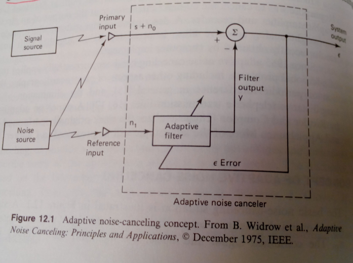
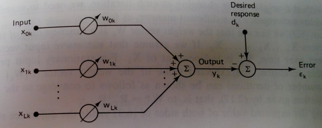
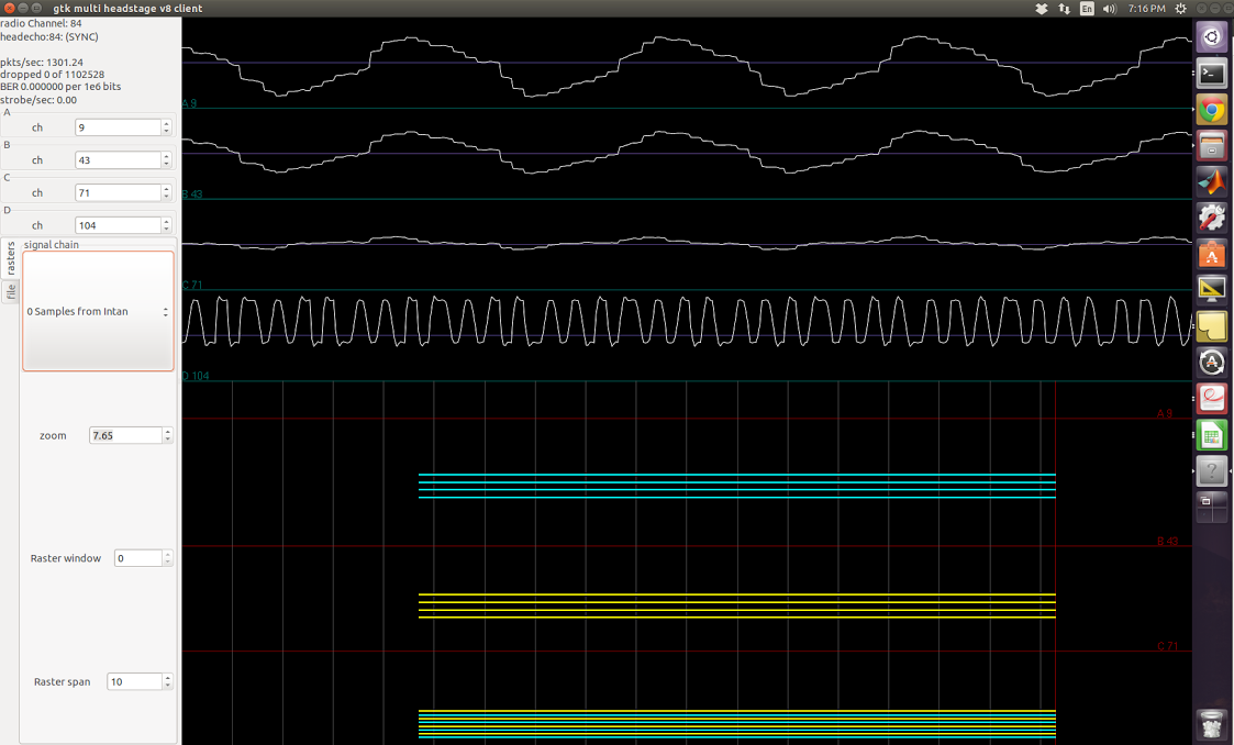
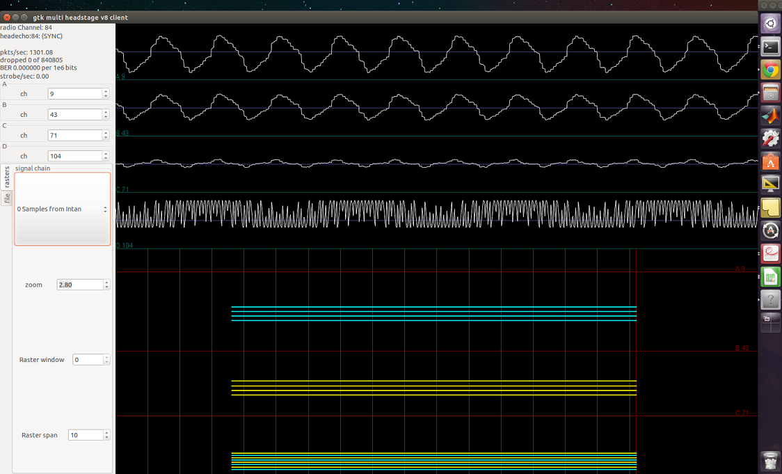
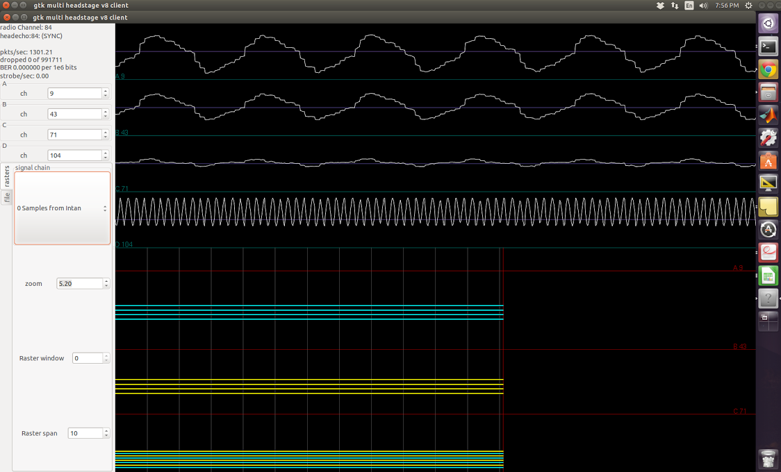
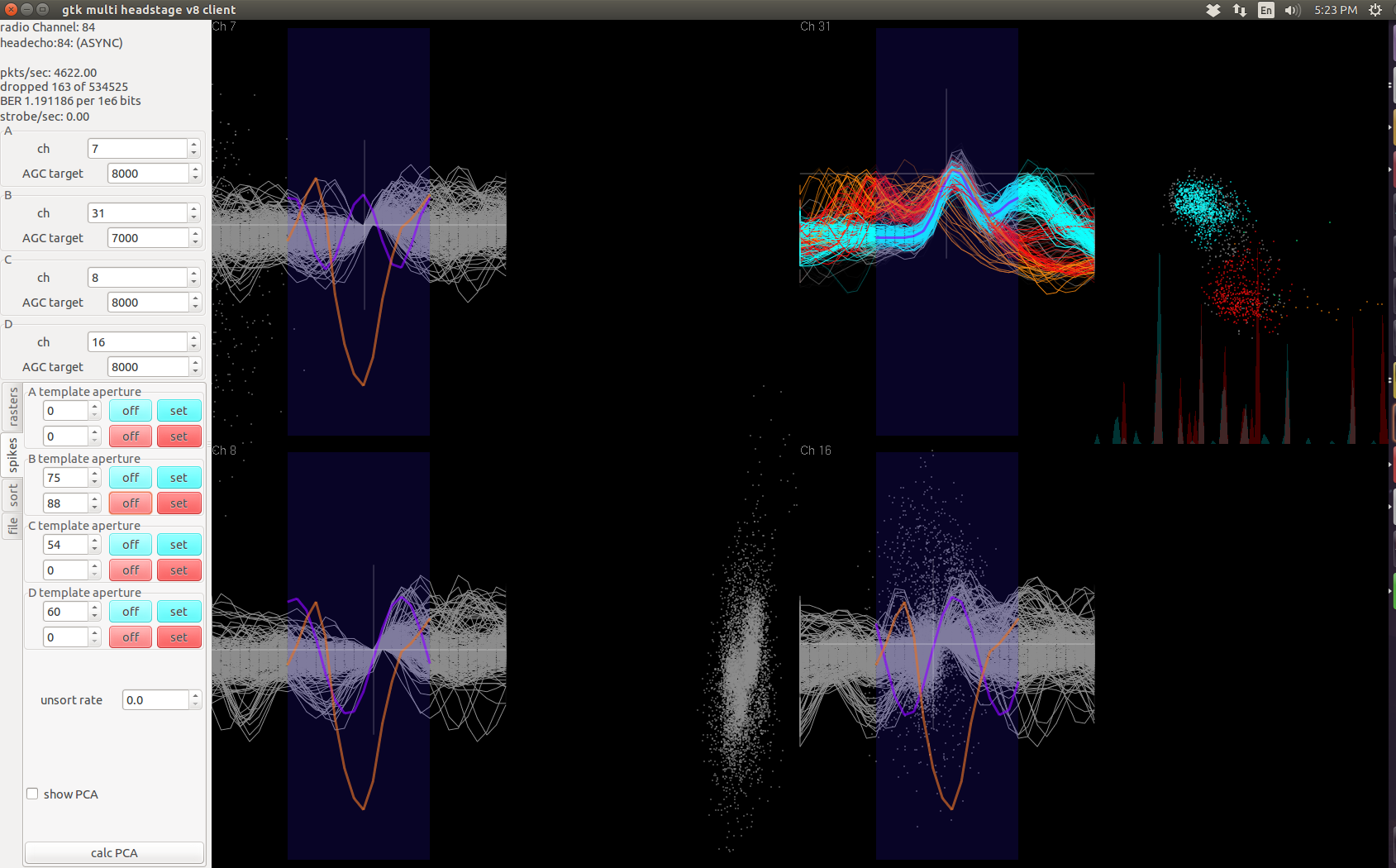
After finishing work on the wireless headstage, it occured to me that no comprehensive validation has been done to confirm spike-sorting and signal quality of the wireless headstages. So I'm conducting a semi-rigourous testing of the RHA-headstage, RHD-headstage, agains the Plexon recordings. This paper on a Blackrock-based wireless system testing has been useful.
First part, I want to examine the signal quality of the streamed raw waveform. The basic setup is:
- Generate a neural signal of known length, save this as an audio signal with sampling frequency Fs=31250Hz. This is chosen because the headstage's sampling frequency is 31250Hz.
- An extra button was added to gtkclient so that as sson as it starts recording the incoming data from the headstages, it also launches VLC to play that audio signal.
- Keep recording until the end of the audio signal.
The recorded signal can then be plotted and analyzed for signal quality.
Note that the command to VLC to play the audio signal is launched from within gtkclient through the system() command. As a result, the headstage is not actually recording that audio signal until after a short VLC initialization delay. This is consistently around 0.5 seconds, as measured by VLC log.
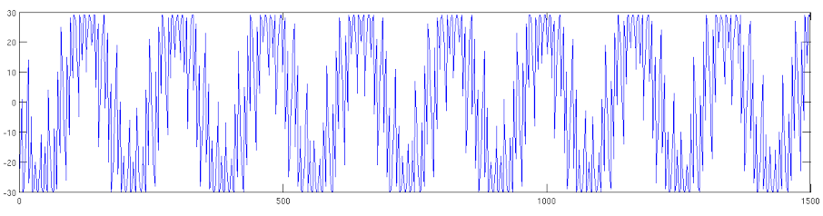
To compare the recorded signal quality against the reference signal, the first test is by visual inspection. Since the recorded signal is a simulated neural signal, this becomes -- do the spike features (sharp peaks and valleys) line up? A more quantitative measure is the cross-correlation between the reference and recorded signals, but the resulting value is a bit harder to interpret.
For the visual test, as a result of the VLC delay, we must shift the recorded waveform to align with the beginning of the reference signal. See below for original signals and aligned signals. Blue is reference, red is recording. The signals are 100 seconds long, with dt=1/31250s.
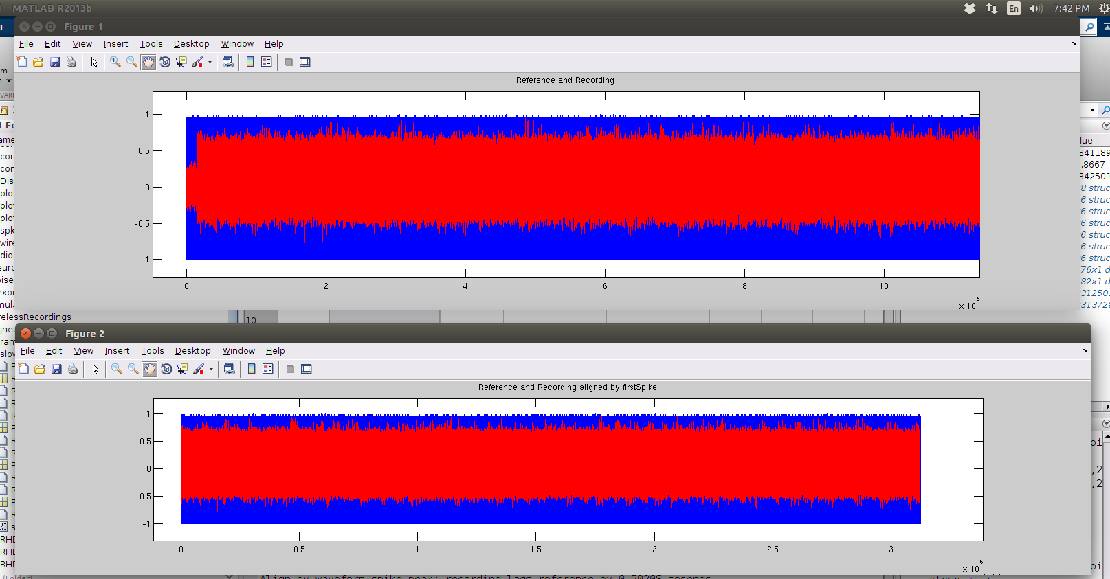
Note the short red segment in the top plot in the beginning, that signals the absence of audio signal.
We can inspect the aligned waveform (by aligning the peak of the first spikes in each signal). In the beginning (shown below), we can see the spike features align fairly well. The squiggles in the red signal are due to noise and filtering artifacts, which are ok in this case but poses the SNR lower limit with which we can distinguish neural signals.
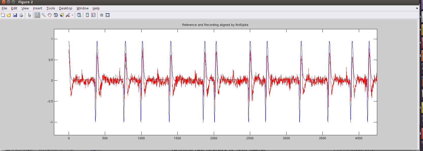
Around the middle of the signal (around 45.82s), we see the signals are no longer aligned. Rough inspections show the red recorded signal has developed a lead over the blue signal - the recording signal has shifted to the left of the reference signal. The three labeled red peaks correspond to the three labeled blue peaks. This is confirmed by the relative time between the labled peaks.
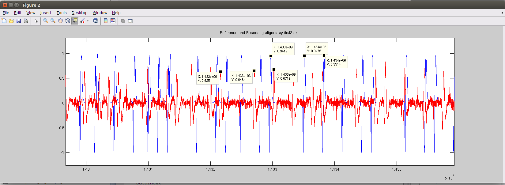
We can further make a table of where the corresponding labeled peaks occur within their respective signals, in terms of sample number:
|Recording samp#       | Ref samp#            | Diff in samp#    | Diff in ms
-----------------------|----------------------|------------------|------------
1432167                | 1432972              | 805              | 25.76
1432707                | 1433515              | 808              | 25.856
1433025                | 1433830              | 805              | 25.76
the last column is calculated by dividing the Diff in samp# by 31250Hz to obtain the lead in seconds, then to ms.
Near the end of the signal (around 96.056s), the lead becomes even greater, as shown below.
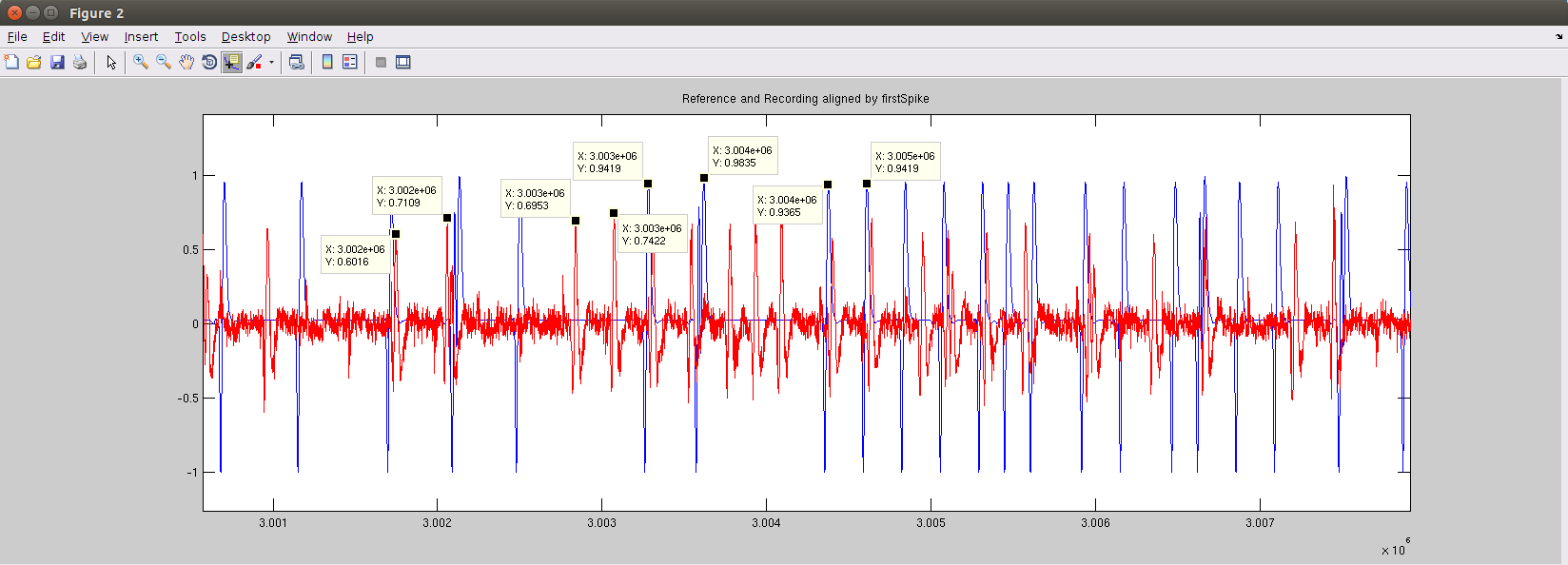
And the corresponding table of labeled peak locations:
|Recording samp#       | Ref samp#            | Diff in samp#    | Diff in ms
-----------------------|----------------------|------------------|------------
3001750                | 3003284              | 1534             | 49.088
3002059                | 3003620              | 1561             | 49.952
3002839                | 3004374              | 1535             | 49.12
3003072                | 3004612              | 1540             | 49.28
The developing lead in sample numbers between the two recorded signals are most likely due to loss of packets from the wireless headstage. Each packet contains new waveform samples, and if they are lost, our recorded signal will be effectively shortened from the reference signal, resulting in this lead. And since the number of lost packets can only increase, this lead will simply increase with time.
While this is a problem when we are doing offline analysis of the recorded signals, it should not be a huge deal in terms of real-time BMI applications where we care about the instantaneous firing rate -- as long as we dont lose too many packets. As Tim has stated in his thesis:
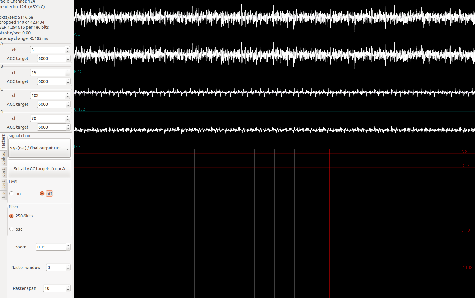
1 in 3176 packets were rejected on average; assuming one bit error per packet, this equates to a bit error rate (BER) of 1.23e-6, or approximately one bit error per second. Efforts to reduce this have not been successful, but the system works acceptably presently.
This matches what I have seen empirically, and comparisons against Plexon. As long as the BER is on the order of 1e-6, then packet loss should not affect performance too much.
The current software keeps track of the total number of lost packets. It might be of interest to find how this changes through time. The previous tables seems to suggest that the number of samples lost increase linearly with time, which supports my hypothesis that the shift is due to last packets. To get a better idea, however, I would want to perform that same analysis around different time points along the signal, probably within a sliding window. Matlab's findpeaks() function can extract the positions of the different peaks within the signals, but matching them would be more difficult. While it is relatively easy via visual inspection, it seems to me to be NP-hard...what's an efficient algorithm to do this?
Update - Perhaps a sliding window of seller's algorithm to match the 'edit distance' of the peaks would answer the question, but that's not too important for our goal of validation.