
Background/Old implementation
We want to be able to acquire signals from as many channels as possible. The original headstage Tim designed has four Intan RHA2132 amplifiers, each of which can amplify signals from 32 channels. Based on signals sent to the chip, the internal multiplexer can be instructed to output the analog signals from any of the 32 channels. These measured voltage signals are then passed to 12-bit ADC running at 1MHz, which means each channel is sampled at about 31.25kHz, standard for neural signal acquisition.
The ADC then sends out the conversion results in a serial interface that is compatible with several standards, such as SPI, QSPI, MICROWIRE, as well as Blackfin’s SPORT interface.
This is great news because with the SPORT interface, there are 4 sets of buses available, meaning the blackfin can talk to four ADCs, and therefore sample from 4 RHA2132 channels at time. Meaning we can sample 128 channels at 31.25kHz each.
Further, since RHA2132 acts as simply analog amplifier, communication between the blackfin and RHA2132+ADC is simple:
- Receive frame sync (RFS) provides the \(\bar{CS}\) signal to the ADC.
- Receive serial clock (RSCLK) provides the SCLK signal to the ADC.
- Receive data lines are connected to the ADC’s data output.
- The input of the ADC connects to MUXout of RHA2132.
- The \(\bar{reset}\) and step signal of all RHA2132 connects to two GPIO pins on the blackfin.
Therefore, at the beginning of each call to DSP-routine, the data values are collected from the SPORT receive buffer. The step line is toggled to step all of the RHA2132’s mux to the next channel. The pin out of this setp is (ADC or amp to blackfin)
- Amplifier 1:
- ADC1 SCLK - RSCLK0
- ADC1 \(\bar{CS}\) - RFS0
- ADC1 DATA - DR0PRI
- Amp1 \(\bar{reset}\) - PF7
- Amp1 step - PF8
- Amplifier 2:
- ADC2 SCLK - RSCLK0
- ADC2 \(\bar{CS}\) - RFS0
- ADC2 DATA - DR0SEC
- Amp2 \(\bar{reset}\) - PF7
- Amp2 step - PF8
- Amplifier 3:
- ADC3 SCLK - RSCLK1
- ADC3 \(\bar{CS}\) - RFS1
- ADC3 DATA - DR1PRI
- Amp3 \(\bar{reset}\) - PF7
- Amp3 step - PF8
- Amplifier 4:
- ADC4 SCLK - RSCLK1
- ADC4 \(\bar{CS}\) - RFS1
- ADC4 DATA - DR1SEC
- Amp4 \(\bar{reset}\) - PF7
- Amp4 step - PF8
Therefore the SPORT ports only receive. SPORT0 generates internal frame sync which becomes the external framesync for SPORT1. The SPORT configurations are (in headstage_firmware/main.c and headstage_firmware/radio5.asm).
1
2
3
4
5
6
7
8
9
SPORT0_RCLKDIV = 1
SPORT0_RFSDIV = 19
SPORT0_RCR1 = 0x0603    // early frame sync, active high RFS, require RFS for every word
SPORT0_RCR2 = 0x010F

SPORT1_RCLKDIV = 1
SPORT1_RFSDIV = 19
SPORT1_RCR1 = 0x0401    // require RFS for every word
SPORT1_RCR2 = 0x010F
The RFSCLK is set to be \(\frac{SCLK}{2x(1+SPORTx\_RCLKDIV)}=\frac{80MHz}{4}=20MHz\). Setting SPORTx_RFSDIV=19 means the ADC’s chip select is pulsed high every 20 SCLK cycles for 1 clock cycle. Therefore the ADC is operated at 1MHz. The ADC outputs 12-bits word. There are 20 clock cycles between each chip-select high pulse, thus there are enough clock cycles for the SPORT to read the data output.
This is straight forward and works well.
New implementation with RHD2132
Intan RHD2132 is essentially RHA2132 with a 16-bit ADC built in. The ADC has maximum sampling frequency of 1MHz, which means when the 32 channels are multiplexed, we can achieve 31.25kHz sampling frequency on each channel.
However, RHD2132 needs to interface with other chips through strictly SPI. This introduces two complications:
-
Instead of simply toggling a pin to reset the amplifier and step the amplifier channel the internal ADC is sampling, each conversion needs to be initiated by a conversion command. This means if we were to keep using the SPORT ports for communication, we have to transmit at the same time as receiving.
-
The SPI timing requirement is shown in the diagram below:
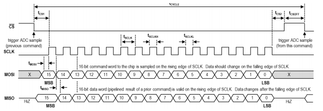
The _CS (\(t_{CS1}\)) high duration needs to be greater than 154ns. The datasheet mentions that the _CS line must be pulsed high between every 16-bit data transfer. Finally, \(t_{CS1}\) and \(t_{CS2}\) must be greater than 20.8ns.
The first modification is easily taken care of – we just need to enable the use of SPORTx_TX ports to send Intan commands at the same time as receiving conversion data.
Fulfilling all of the SPI timing requirements is impossible with the SPORT interface because:
RHD2132 transmits and receives only when _CS is pulled low. That means both RFSync and TFSync which dictates when a 16-bits word is received by or transmited from the blackfin, must be connected to _CS, and have the same timing. This was easily done by having TFSync to be internally generated, and set RFSync as externally generated and receives TFSync. The RSCLKx and TSCLKx, which dictates when a bit is sampled or driven out onto the bus is edge-sync’d to the RFSync and TFSync signal, respectively. At the same time, RSCLKx and TSCLKx have to be set to have the same timing, and connects to RHD2132’s SCLK.
The new Blackin SPORT to RHD2132 amplifiers connections are (amplifiers numbered from left to right):
- Amplifier 1: SPORT1_SEC
- SCLK+ to SCLK1
- \(\bar{cs+}\) to FSync1
- MOSI+ to DT1SEC
- MISO+ to DR1SEC
- Amplifier 2: SPORT1_PRI
- SCLK+ to SCLK1
- \(\bar{cs+}\) to FSync1
- MOSI+ to DT1PRI
- MISO+ to DR1PRI
- Amplifier 3: SPORT0_SEC
- SCLK+ to SCLK0
- \(\bar{cs+}\) to FSync0
- MOSI+ to DT0SEC
- MISO+ to DR0SEC
- Amplifier 4: SPORT0_PRI
- SCLK+ to SCLK0
- \(\bar{cs+}\) to FSync0
- MOSI+ to DT0PRI
- MISO+ to DR0PRI
where SCLK0 is RSCLK0 and TSCLK0 tied together, SCLK1 is RSCLK1 and TSCLK1 tied together, FSync0 is RFS0 and TFS0 tied together, and FSync1 is RFS1 and TFS1 tied together.
This means the falling edge of _CS always corresponds to either the falling/rising edge of SCLK, and similarly, the rising edge of _CS corresponds to either the falling/rising edge of SCLK. However, \(t_{CS1}\) defines the timing between falling edge of _CS and the next rising edge of SCLK, while \(t_{CS2}\) defines the timing between falling edge of _CS and the next rising edge of SCLK. Given the operation of SPORT, one of these requirements will be violated.
In fact, according to ADI engineers, it is not possible to fulfill all the timing requirements when using SPORT to emulate SPI. So I just hoped it could work anyways and tried to test this.
Testing
My final SPORT settings are, collected from headstage2_firmware/main.c and headstage2_firmware/intan_setup_test.asm (but also other firmware versions. intan_setup_test is simply the first time I tested them):
1
2
3
4
5
6
7
8
9
10
11
12
13
14
15
16
17
18
19
20
21
22
// SPORT0 transmit
// Using TCLK for late-frame sync
SPORT0_TCLKDIV = 1;
SPORT0_TFSDIV = 3;
SPORT0_TCR2 = TXSE | 0x10;  // allow secondary, 17 bits word
SPORT0_TCR1 = TCKFE | LATFS | LTFS | TFSR | ITFS | ITCLK | TSPEN | DITFS;

// SPORT1 transmit
SPORT1_TCLKDIV = 1;
SPORT1_TFSDIV = 3;
SPORT1_TCR2 = TXSE | 0x10;  // allow secondary, 17 bits word
SPORT1_TCR1 = TCKFE | LATFS | LTFS | TFSR | ITFS | ITCLK | TSPEN | DITFS;

// SPORT0 receive
// Serial clock and frame syncs derived from TSCLK and TFS, so RCLKDIV and RFSDIV ignored
SPORT0_RCR2 = RXSE | 0x10;  // allow secondary, 17 bits word
SPORT0_RCR1 = RCKFE | LARFS | LRFS | RFSR | RSPEN;

// SPORT1 receive
// Serial clock and frame syncs derived from TSCLK and TFS, so RCLKDIV and RFSDIV ignored
SPORT1_RCR2 = RXSE | 0x010; // allow secondary, 17 bits word
SPORT1_RCR1 = RCKFE | LARFS | LRFS | RFSR | RSPEN;
In this setup, the receive clock and frame sync are the same as the transmit clock and frame sync. The TSCLK=RSCLK=SCLK of RHD2132, is again set to be 20MHz.
LTFS sets the frame sync signal to be active low.
SPORTx_TFSDIV=3 would mean the frame sync or _CS is pulled low for 1 SCLK (50ns) every 4 cycles (200ns).
However, LATFS sets late frame sync, which means when a frame sync triggers transmission or reception of a word, it will stay low during that time, and another further frame-sync during this time is ignored by the SPORT. After that time, if it’s not time for another frame sync yet, frame sync will return to high, otherwise, it will be low again. Late frame sync also means the timing requiring between the falling edge of _CS and the next rising edge of SCLK is fulfilled.
Together, this means _CS will be low for 17 SCLK cycles, or \(17\times50ns=850ns\) while high for 3 SCLK cycles, or \(3\times50ns=150ns\). This is because, when frame sync first goes low, it will stay low for 17 SCLK cycles, at which time it will go high because 17 is not a multiple of 4. The next greatest multiple of 4 is 20, which is when frame sync will be pulled low again.
The reason for _CS to be low for 17 SCLK cycles is two fold:
-
Because a dataword is 16 bits, it has to be at least greater than 16 cycles. No matter what settings I have, the \(t_{cs2}\) requirment will be violated, which based on how multiplexer work, will affect the value of the last bit being read. Since the data is read MSBit first, having 17 clock cycles would mean only the 17th bit, which I will discard later will be corrupted by the \(t_{cs2}\) violation. Therefore no harm done!
-
With _CS low for 17 cycles and high for 3 cycles, I get exactly 20 cycles period, making it 1MHz. This is one of the only configurations that allows me to achieve that.
With this setup, the \(t_{cs2}\) timing requirement is not fulfilled at all, while \(t_{csoff}\) is violated by 4ns.
Initial testing required checking the acquired sample values. Fortunately, all RHD2132 comes with registers that contains the ASCII values of ‘I’, ‘N’, ‘T’, ‘A’, ‘N’. Therefore, if the SPI emulation actually works, I can just issue READ commands of those register locations to Intan, and check whether the received results are correct.
One thing to remember is that when a command to convert a channel is sent, the conversion result is not received until two SPORT cycles later. This also means, if the pipeline is full, when you stop sending commands, it takes two cycles for the pipeline to be completely empty of new data. But since with the SPORT setup, we can’t read from Intan without also sending, that means the last (old) command will have to be send three times during the time it takes to clear the pipeline.
After establishing that, I then needed to make sure I can sample and obtain correct waveforms. This is done by applying a sinusoid of known frequency to the amplifier. In the firmware, I would simply read the the channels four at a time (ch1 on all four amps, then ch2 on all four amps, so on), while sending commands to tell the amplifiers to convert the next channels at the same time as reading. I would save the sample read from the same amplifier every time.
Running this test program (first version is headstage2_firmware/intan_setup_test.asm) and setting breakpoint at the end of execution through JTAG, I can dump the saved data and plot them (using headstage2_firmware/plot_memdump.py).
Initial test result for all 32 channels of amplifier 1, when the first channel is applied a 6400Hz signal looks like below:
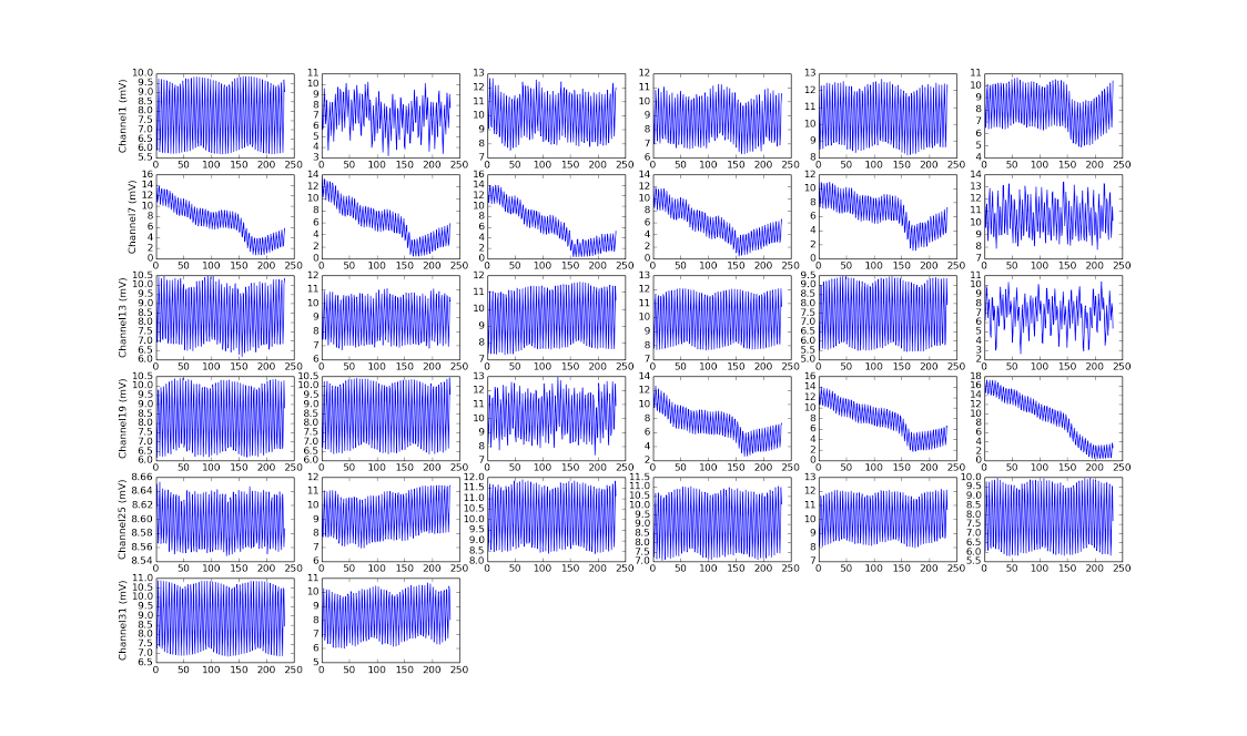
I have signal, but it’s not what I expected at all…channels without signals are oscillating, there were too many cycles, etc.
This is strange because when I repeatedly convert just one channel using the same setup (sending CONVERT(0), CONVERT(0)…) rather than converting each channel in turn (sending CONVERT(0), CONVERT(1), CONVERT(2),…), I get great result:
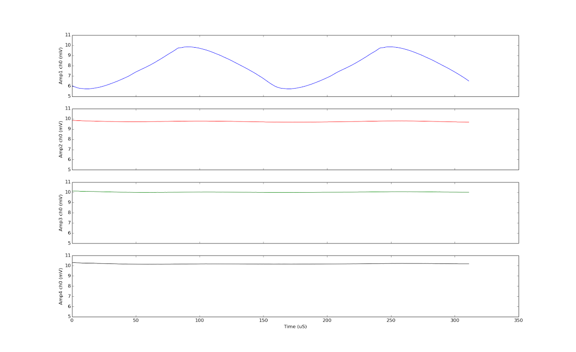
I got two periods on the first channel of amplifier 1. The bottom 3 are the first channels of the other amplifiers, which are quiet as expected.
Turns out the difference is due to reduce sampling frequency. In the second case, where the sampling frequency is 1MHz, each period of 6400Hz wave would require 156 samples.
However, while calculating how many samples I needed to collect in the first case, I mistakenly used the 156 samples/value. When I sample 32 channels round-robin style, the effective sampling rate applied to each channel is 31.25kHz, that means only 5 samples/period is needed. This is why my plots had way more periods than expected.
Secondly, the channels that weren’t applied signals were left floating. This means it’s susceptible to all the noise within the amplifier and PCB planes, resulting in same oscillation frequency, but different amplitude and DC value.
After calculating the correct number of samples to collect to see 2 periods of 6400Hz on all 32 channels of an amplifier, and correctly grounding the channels without applied signals, and turning on Intan’s DSP highpass filter/offset removal, the results then looked just as expected:
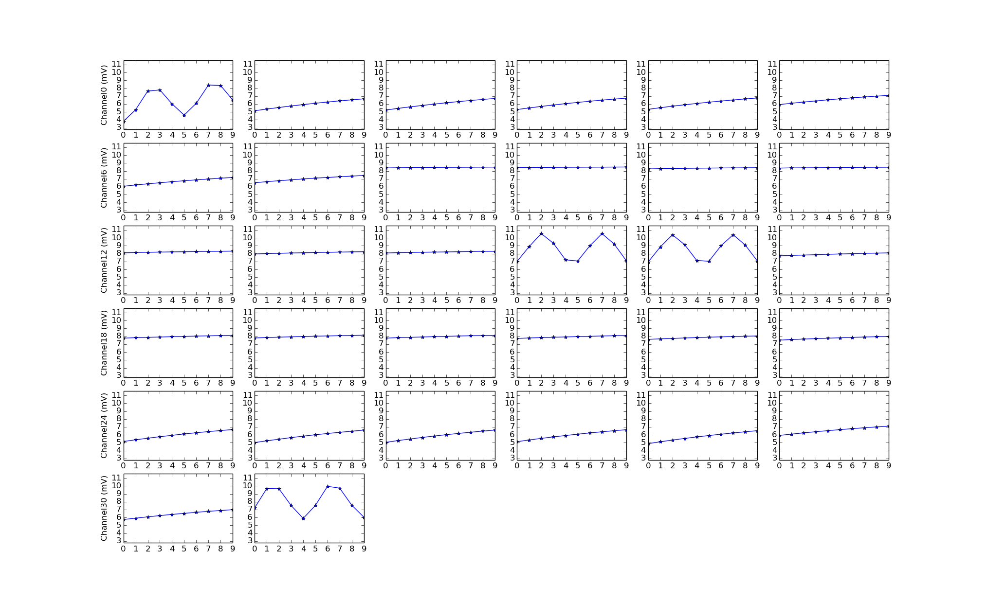
In the plot above, channel 0, 15, 31 and 16 are applied the 6400Hz signal while the others are grounded.
Consequences of the new configuration
RHD2132 also support outputting ADC results in either unsigned offset-binary where reference electrode voltage has the value of 0x8000, or using signed two’s complement, where the reference electrode has the value of 0x0000 and values less than that has the MSB set to 1 two’s complement style.
This would result in modifications of the first stage of the firmware’s signal chain, which is to convert the incoming samples to fixed-point Q1.15 format for further processing. See the post on modifying the AGC stage.
Finally, the option DITFS make the SPORT frame-sync, read and write happen every \(1\mu s\) regardless if new commands have been pushed into the SPORT transmit FIFO. This means, if our code-path (signal-chain plus the radio transmission code) inbetween SPORT FIFO reads/writes is too long, the previous command in the FIFO will be sent again, and two cycles later, the corresponding result will be read. This will then result in erroneous data.
However, the manifestation of this data corruption is somewhat counter-intuitive. After establishing correct Intan and SPORT setup to successfully acquire signals, I added in minimally modified signal-chain code from RHA-headstage’s working firmware headstage_firmware/radio5.asm, and saved all pre-processed samples from one of the amplifiers in memory (headstage2_firmware/firmware1.asm). I then stopped the execution when the designated buffer is memory is full, dumped the results for plotting in JTAG. The plots, which I expected to be smooth sinusoids of the applied signal, were riddled with random spikes.
This cannot be due to the signal-chain code since the samples saved came directly from the SPORT. A second test where I simply added nops inbetween SPORT reads/writes confirms that the data corruption was due to the code-path being too long. However, the number of nops that allowed for glitchless data acquisition is less than the signal-chain length used in radio5.asm. This is very strange, since the timing requirement for both headstage firmware setup is similar – accounting for the radio transmission code, the DSP code has to finish in about 800ns. But somehow the timing budget for the RHD-headstage is significantly less.
In the nop test done in firmware2.asm, it was found I can fit 150 nops. I have yet to figure out why this is the case. Regardless, that means a reduction of the original RHA-headstage firmware is needed to adapt it to RHD-headstage. Since the radio-transmission code must stay the same, this reduction is exclusively on the signal-chain code, which includes:
-
high-pass + AGC = 5 cycles/2 channels * 2 = 10 cycles.
In each signal-chain iteration 4 samples are acquired, 1 per amplifier, so all 4 must be processed. Blackfin works efficiently with two 16-bit samples at once, so samples from two channels are processed first, then the remaining two samples are processed in the rest of the signal-chain code.
-
LMS = 27 cycles/2 channels * 2 = 54 cycles.
-
IIR = 27 cycles/2 channels * 2 = 54 cycles.
-
SAA = 58 cycles.
AGC is automatic gain control, LMS is least-mean-square adaptive noise cancellation, IIR is infinite impulse response filter, and SAA is used for spike template matching.
Among these, SAA is required for spike matching. AGC is required because the templates for spike-sorting were made under certain signal power level, AGC is needed to fix the channel’s power level. Therefore, all of LMS and half of IIR are ripped out to reduce code-length.
Update: 7/26/2017
The reduction of available processing cycles kept bothering me, so I tried to see what it is caused by and how I can squeeze more cycles.
Initial RHD-headstage firmware flows like so:
-
Initialize all memory bank values
_radio_bidi_asm. -
Setup Intan communication by writing to its config registers and calibrate the ADC
comm_setup. -
Go to main loop where signal acquistion and processing interleaves with radio transmission.
In step 3, after getting the latest samples from the SPORT buffers, we increment the channel count, construct a proper request to Intan and send it through SPORT again. The SPORT would presumable output this to Intan headstages simulataneously while reading for new samples from Intan. This is done through:
1
2
3
4
5
r7 = CHANNEL_SHIFTED;
[p0 + (SPORT1_TX - SPORT0_RX)] = r7;   // SPORT1 primary TX
[p0 + (SPORT1_TX - SPORT0_RX)] = r7;   // SPORT1 sec TX
[p0 + (SPORT0_TX - SPORT0_RX)] = r7;   // SPORT0 primary TX
[p0 + (SPORT0_TX - SPORT0_RX)] = r7;   // SPORT0 sec TX
Turns out if in the Intan-setup phase, prior to the start of signal acquisition, I leave the command for auto-incrementing selected amplifier channel in the SPORT transmission (SPORT1_TX, SPORT0_TX) and delete the above snippet from the signal acquisition code, the same behavior is achieved and I can an extra 57 cycles to work with during step 3. This then allows me to fit the entire LMS step into the firmware.
Why does this happen? Probably because accessing the SPORT ports on the blackfin, takes more than 1 CCLK cycle (1/400MHz=2.5ns), which is the case for all the instructions. The ADSP-BF532 hardware reference section 3-5 mentions that Peripheral Access Bus (PAB) and Memory Mapped Register (MMR) access, which includes SPORTx_TX and SPORTx_RX takes 2 SCLK cycles.
SCLK cycle is set to 80MHz, which is 5 CCLK cycles. The code snippet above takes 4*2=8 SCLK cycles, or 40 CCLK cycles. This is less than the extra 57 cycles I got after deleting them, but I think confirms what I see.